
Observation and Measurement of Semiconductor Wafers and IC Designs Using Microscopes
There has been intense competition in the semiconductor industry to produce smaller and more functional products, improve productivity, and reduce costs. In response to increasingly smaller designs and larger diameter wafers, more advanced quality assurance and even faster R&D and inspection continue to be required.
This section introduces new application examples of KEYENCE’s latest 4K Digital Microscope, which makes the conventional inspections in the semiconductor industry much more advanced and efficient.

- Larger Diameter Wafers and New Requirements
- Inspection of Wafers and IC Designs
- Latest Solutions for Inspection of Wafers and IC Designs
- VHX系列是半导体行业的新型合作伙伴
Larger Diameter Wafers and New Requirements
晶圆制造年代是不可或缺的emiconductors. To be used in increasingly smaller devices, semiconductor products are required to be more compact, but have higher functionality and quality. To manufacture value-added products effectively, many manufacturers are competing against each other in the areas of research and development, development of manufacturing technologies, and quality control.
One popular example to increase productivity is to produce larger diameter silicon wafers so as to produce more chips from a single wafer. The production of larger diameter wafers has been studied for many years to meet various requirements such as reduced loss due to defects, higher flatness, and lower costs. To produce larger and flatter wafers, double side polishing is considered to have advantages over single side polishing, and thus double side polished wafers with a diameter of 12 inches are most widely produced. Wafers with a diameter larger than 12 inches have appeared in recent years, and wafers with a diameter of 15 inches or even larger are expected to be produced in the future. To ensure stable quality of such wafers and further increase productivity of IC chips, constant research and development is crucial.
The popular circuit patterning technologies include high-definition screen printing, which efficiently prints patterns fine enough to be used in micro-electromechanical systems (MEMS), and inkjet coating , which enables efficient small-volume manufacturing of many product types. Because these components are so critical, advanced inspection and evaluation is required.
Inspection of Wafers and IC Designs
在半导体制造中,即使是极小的缺陷和外国颗粒也会引起性能问题。晶片通常由装载机转移,并使用多种不同的仪器进行检查,包括光学显微镜和扫描电子显微镜(SEMS)。但是,市场上的激烈竞争以及越来越小的功能导致了检查速度和准确性的提高。
Problems with conventional observation instruments
- Optical microscope
- Resolution is not high enough to observe small features at high magnification.
- Inspecting for foreign particles is time consuming
- 观察角度是固定的,这使得它的小鬼ossible to observe the edges of a wafer.
- Measurement is not supported and thus targets need to be moved to another inspection device and positioned again for measurement, which increases the number of steps in the inspection procedure.
- Scanning electron microscope (SEM)
- The sample must undergo sample preparation in a vacuum chamber.
- Monochrome images are obtained, limiting inspection capabilities.
Latest Solutions for Inspection of Wafers and IC Designs
For the past 20 years, KEYENCE has repeatedly improved its digital microscopes using direct customer feedback. The latest VHX Series uses improved functionality and 4K imaging to overcome problems seen with conventional microscopes and SEMs.
This section introduces inspection examples of wafers and integrated circuits using the VHX Series 4K Digital Microscope. All examples introduced here use a single VHX Series unit.
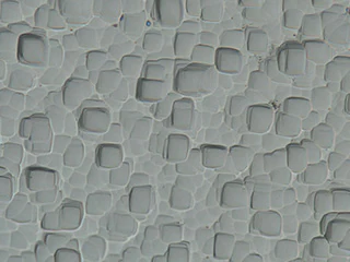
Observation of wafers using 4K optical shadow effect mode
Using a specialized design featuring a high-resolution HR lens, a 4K CMOS image sensor, and lighting technology, the VHX Series 4K Digital Microscope has achieved a whole new method of microscopy, “Optical Shadow Effect Mode.”
The multi-directional lighting variation method analyzes the contrast on the image captured with varied illumination, allowing users to detect subtle irregularities on a target. The images captured using Optical Shadow Effect Mode rival those of an SEM, but require no sample preparation.
颜色信息可以覆盖在光阴影效果模式图像上,从而可以同时表示表面和颜色信息。


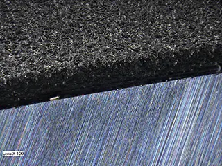
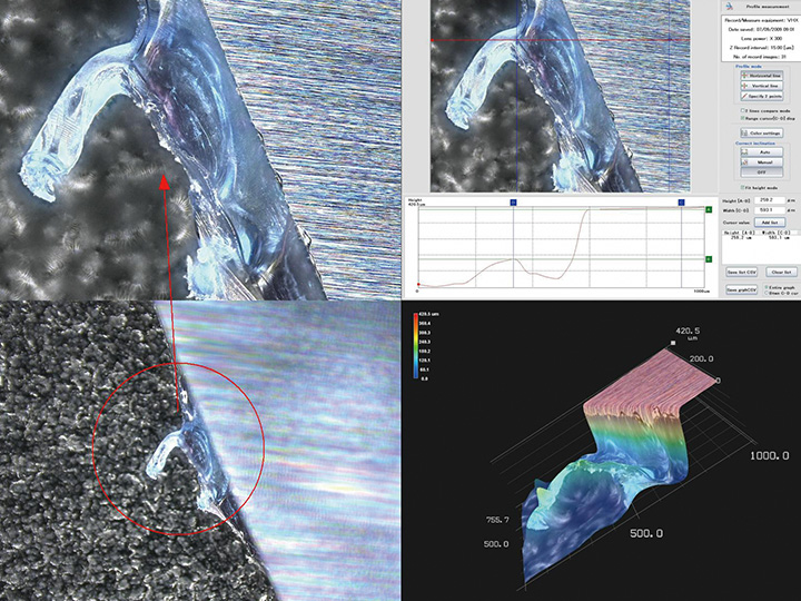
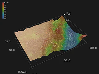
观察和测量晶片边缘
The free-angle observation system of the VHX Series 4K Digital Microscope enables tilted observation of wafer edges.
The deep depth of field and the real-time depth composition make it possible to obtain clear 4K images that fully focus on the entire surface, edges, and defective areas of a wafer even at high magnification.
The created high-resolution magnified image can also be used for highly accurate 2D measurement and 3D shape and profile measurements of defective areas. These measurements make it possible to complete procedures quickly and seamlessly with a single unit.

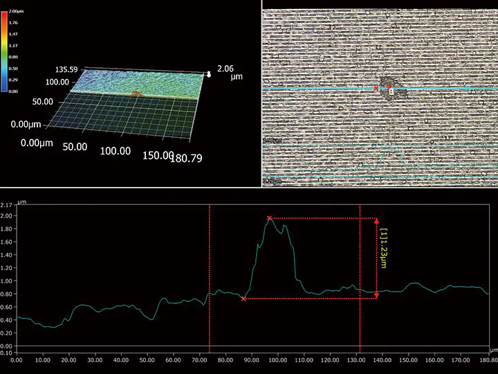
Observation and analysis of defects that occur in wafer processing
The VHX Series 4K Digital Microscope has a depth of field that is 20 times greater than that of conventional microscopes. In addition, its high-dynamic-range (HDR) imaging function captures multiple images at varying shutter speeds to obtain an image with high color gradation and contrast. Microscopic defects can be analyzed even on highly reflective surfaces with little contrast.
3D imaging enables the surface shape to be visualized, and profiles can be measured across defects on the surface. Furthermore, the automatic area measurement tools allows for photomasking to be quickly measured and reported, dramatically improving work efficiency.


观察和3D形状测量粘附在晶圆上的外国颗粒
The VHX Series 4K Digital Microscope supports high magnification imaging, up to 6000x. The auto area function enables contamination analysis to be performed with just a few clicks. After identifying foreign particles, 3D images can be taken to further understand their size and shape.
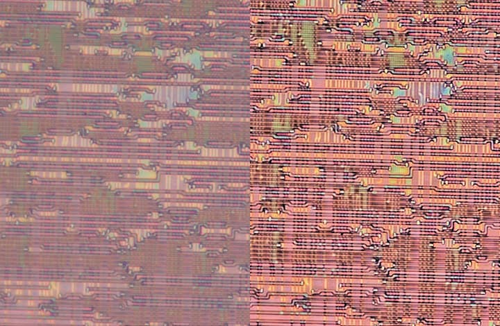
High-resolution observation of integrated circuits
The VHX Series 4K Digital Microscope is equipped with a high-resolution HR lens and a 4K CMOS to enable high-resolution imaging. In high-magnification observation of IC patterns using normal microscopes, there were cases where clear images could not be obtained due to insufficient resolution. With the VHX Series, such microscopic IC patterns can be observed with a high-resolution 4K image.
Full integrated circuit inspection
The high-resolution HR lens and motorized revolver of the VHX Series 4K Digital Microscope enable a seamless zoom function that automatically switches lenses from 20x to 6000x magnification with intuitive operations.
At the push of a button, high speed image stitching automatically captures 4K images with no misalignment, providing a fully focused image over a large area. With a simple click, users can zoom in on features of interest using the fully automated XY stage.


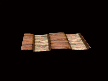
3D shape measurement of integrated circuits
The VHX Series 4K Digital Microscope instantly creates a fully focused 3D image of an integrated circuit. When displayed in 3D, the IC pattern surfaces can be observed freely from various angles.
High-accuracy profile measurement can also be performed using the obtained height data, significantly improving inspection accuracy and work efficiency.
VHX系列是半导体行业的新型合作伙伴
除此处介绍的功能外,VHX系列高清4K数字显微镜还配备了许多有用的研究,开发和制造地点的功能。对于半导体晶片和集成电路,一个单元可以识别缺陷,捕获图像,执行2D和3D测量,并自动创建报告。
Advanced automatic control and image processing allow even beginners to capture clear 4K images quickly with simple operations. This dramatically improves both inspection accuracy and work speed.
有关其他产品信息或查询,请单击下面的按钮。
