
Inspection and Measurement of Solder Cracks and Voids
PCBs and electronic components are becoming smaller and denser, requiring higher quality soldering to mount these components. Analysis of solder defects are especially important for the automotive industry, where advanced computerized control is increasing rapidly.
This section mainly introduces the latest examples of microscopic observation of typical solder defects, such as solder cracks and solder voids, using KEYENCE's latest 4K Digital Microscope.
- Changes in the Environment Surrounding Solder
- 焊接缺陷和观察焊接的重要性Cracks and Solder Voids
- Latest Examples of Observation and Analysis of Solder Cracks and Solder Voids
- 一个具有所有功能的单位,对于焊料的质量保证必不可少
Changes in the Environment Surrounding Solder
智能手机,平板电脑和可穿戴设备的功能更大,更小且更薄。为了使此类设备成为可能,更小,更分层的PCB已变得普遍。
In the automotive industry, autobraking and autonomous driving require advanced computerized control of the car; because of this, PCBs and other electronic components must be even more durable and reliable.
焊料在电子连续性和电子组件之间的连接中起关键作用,因此特别需要具有更高的耐用性和可靠性。此外,始于2000年代的无铅焊料的使用增加了对粘结技术的需求,以防止材料的覆盖。
Reliability evaluation tests are those tests that are indispensable in the evaluation of the durability and reliability of solder. Among these tests, temperature cycle tests are typically used for evaluating solder.
There are various solder defects that can cause problems. One example is caused by insufficient solder wettability* of solder paste that is automatically applied to a metal plate and printed. Such solder, in concave parts, can decrease bond strength to a solder pad or cause defects such as solder voids. To improve quality, it is essential to use observation and analysis to identify the causes of solder defects. The next section explains typical solder defects, the risks that these defects present, and the necessity of observation.
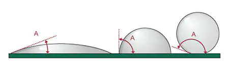
焊接性在固体表面和液体(例如,熔化的焊料)之间的接触角表示。图像中的角度A(接触角θ)的越小,焊料可湿性越高,表明液体被广泛应用于固体表面的情况。接触角越大,焊料润湿性越低,则表明固体表面排斥施加液体的情况。
焊接缺陷和观察焊接的重要性Cracks and Solder Voids
Typical solder defects include "solder bridges and "excessive solder" in which too much solder causes short-circuiting. Additionally, "solder splatter" occurs due to excessive heating, while "cold solder joints" occur due to insufficient heating.
There are also “solder cracks” and “solder voids,” which are difficult to detect and identify the causes immediately after mounting. These defects can be caused by various factors and, not only immediately after solder bonds are formed, they can occur or progress over time or due to stress. Therefore, these defects need to be observed and analyzed with microscopes or other measuring instruments.
- Causes and risks of solder cracks
- Solder cracks occur or progress due to factors such as fatigue, the passage of time, and the application of stress after solder bonds are formed. If cracks that are microscopic during the initial stages of packaging grow, the resistance of the bond will increase. There are even cases where solder cracks lead to Joule heating. Grown cracks can also completely separate the bond, leading to a component failure. In particular, cracks in lead-free solder are said to progress rapidly once they form. Since grown solder cracks can generate heat and cause fire, they need careful inspection.
- Causes and risks of solder voids
- 焊接空隙主要是由焊料中包含的气泡引起的,这些气泡在焊料回流的印刷过程中应用,在组件安装过程中生成的气体以及用于凹入零件的焊料糊状物的焊料可检湿性不足。焊接可以降低焊料强度,部分降低的强度会导致焊接裂纹。这就是为什么引起焊料空隙和对此原因的对策非常重要的原因。
为了确保质量和改善过程,重要的是要观察,分析和评估故障产品中的焊料裂缝和空隙。
Latest Examples of Observation and Analysis of Solder Cracks and Solder Voids
Applied solder is three-dimensional, but conventional microscopes only focus on part of it in high-magnification observation due to an insufficient depth of field. Hence, delicate focusing for each part of the observation target is necessary.
Conventional microscopes also do not fully focus on targets having surface irregularities caused by insufficient polishing. Other conventional problems include undetected defects due to reflection from glossy materials and initial subtle cracks that cannot be observed at high magnification or due to insufficient resolution.
KEYENCE’s VHX Series high-definition 4K Digital Microscope can solve these conventional problems, with the high-resolution optical system having a deep depth of field, the 4K CMOS image sensor, and specially designed systems such as high-performance lighting and advanced image processing. More advanced observation, defect analysis, and evaluation of solder can be performed quickly with simple operations, significantly improving work efficiency.
This section introduces the latest examples of observation and analysis of solder defects using the VHX Series.
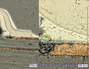
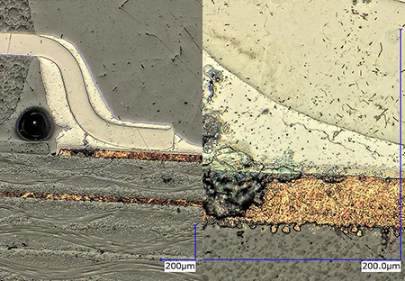
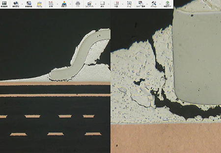
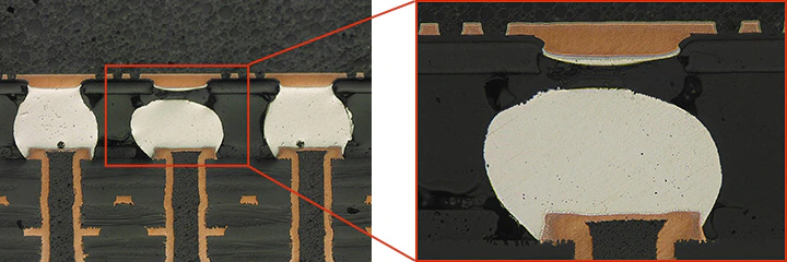
Tilted observation of solder cracks on packaged PCBs
The free-angle observation system of the VHX Series 4K Digital Microscope enables tilted observation of three-dimensional solder fillets on packaged PCBs.
Furthermore, its glare removal function and ring-reflection removal function enable solder crack observations that are both clear and unaffected by solder-specific reflected light.
The VHX Series has achieved a depth of field that is approximately 20 times deeper than that of conventional microscopes. Real-time depth composition is also available and easily creates clear 4K images that fully focus on the entire target, even at high magnification.


Left: depth composition, glare removal, ring-reflection removal/right: normal

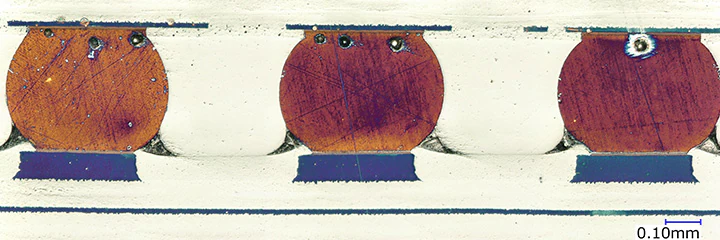
观察of solder cracks on cross sections of electronic components
Solder cracks that are initially microscopic can grow over time, leading to component failures, heat generation, and fire. Overlooking fine cracks due to insufficient magnification or resolution has been a serious issue.
The high-resolution HR lens and motorized revolver of the VHX Series 4K Digital Microscope enable a seamless zoom function that automatically switches lenses from 20x to 6000x magnification with intuitive operations. A high-magnification image of a defective area can be displayed next to a low-magnification image using the split screen function, allowing users to always track what they are viewing during high-magnification observation.
Furthermore, with a deep depth of field and real-time depth composition, submicron cracks can be observed with a clear image, even if there are surface irregularities.
观察of solder voids on cross section samples
The VHX Series 4K Digital Microscope provides fully focused images of cross-sections, even if there are irregularities introduced by insufficient polishing. These images enable high-resolution observation without any voids being overlooked.
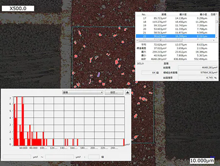
Quantitative analysis of PCB cross sections
The VHX Series 4K Digital Microscope enables high-accuracy automatic area measurement and counting with a high-resolution magnified image. These functions allow users to perform quantitative analysis and generate reports with a single unit, significantly improving efficiency.

Evaluation of bond strength based on solder fillet appearance
With conventional microscopes, lighting is difficult to set due to the reflection from solder surfaces, causing variations in results among operators.
With the multi-lighting function of the VHX Series 4K Digital Microscope, omnidirectional lighting data is automatically captured with the push of a button.
The most suitable image to use in observation and evaluation can be selected from among the images captured with the multi-lighting function, thereby significantly reducing the time conventionally required for light adjustment. Image data with different lighting is automatically saved, so other images with different lighting conditions can be loaded immediately.
Furthermore, using the glare removal function and ring-reflection removal function suppresses solder-specific reflected light, enabling observations of solder joint appearances with a clear image.

一个具有所有功能的单位,对于焊料的质量保证必不可少
The VHX Series 4K Digital Microscope has many other functions, such as 2D and 3D measurements, and enables observation, analysis, measurement, and reporting to be performed with a single unit.
有关其他产品信息或查询,请单击下面的按钮。
